Microsystem technology

Small technology on a very large scale

Microelectronics is a classic cross-sectional technology across all subject areas: Whether in automation, communication technology, optics, medical technology or networked assistance systems - sensors and microsystems are universally applicable, electronic processes take place in ever-smaller spaces.

Integrated Assembly

Production of mobile systems without assembly

In stereolithography, the components are placed in prepared cavities during layer-by-layer deposition. The required contacting is achieved by sequential deposition methods at low temperatures. After curing of the materials, an individual prototype with optimally adapted form factors is created. The special feature of this process is the possibility of individually integrating sensors, actuators, fluidic and optical conductors by adapting CAD data. The combination with so-called sacrificial layers even allows internal components such as rollers, gear wheels or simple mechanisms to be kept movable without assembly. 

Electronic Embedding

Integration of additional electronic functions in components

The demands on microsystems technology and so-called heterointegration are constantly increasing to meet the needs of the population. Such functional microelectronic systems can, for example, be completely adapted to the patient's needs as prostheses or fill existing installation space with micrometer precision. The individual production of such complex units is no longer a utopia thanks to the combination of stereolithography and multi-jet modeling with microsystem technologies. Keyboards, displays, microcontrollers and the sensor-actuator periphery can be combined to individualized embedded systems using embedding techniques.


Integration of RFID chips

Thanks to rapid manufacturing, radio chips can even be integrated into metallic components. Researchers at the Fraunhofer Institute developed the process for Manufacturing Technology and Applied Materials Research IFAM in Bremen. The "intelligent" metal components are fitted with RFID chips in just one work step. The three-dimensional CAD model from the computer is built up layer by layer by a machine as a prototype. The Fraunhofer scientists can control this process so that the built-in RFID chip is completely enclosed by the material.
Project examples

Intelligent sensor systems

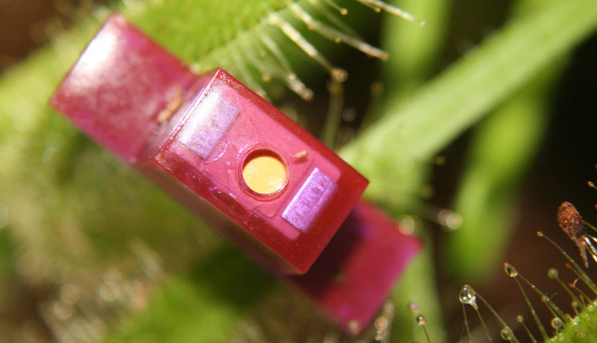
A new moisture sensor was developed at the Fraunhofer IZM site in Oberpfaffenhofen: This intelligent sensor system, which is manufactured entirely by additive processes, can be individually adapted to external mechanical requirements. Three-dimensional methods have a very large future potential for fulfilling the individual requirements of end customers. Efficient software tools significantly improved the adaptation of the electronic functionalities. The reliable integration and contacting of microsystem components is crucial.

The scientists at Fraunhofer IZM are researching further integration methods with which the smallest electronic structures can be safely integrated and connected.